Phase-Locked Loop (PLL)
Phase-Locked Loop (PLL). EE174 – SJSU Tan Nguyen. OBJECTIVES. Introduction to Phase-locked loop (PLL) Historical Background Basic PLL System Phase Detector (PD) Voltage Controlled Oscillator (VCO) Loop Filter (LF) PLL Applications. Introduction to Phase-locked Loop (PLL).
Share Presentation
Embed Code
Link
Download Presentation
- frequency
- put frequency
- digital pll
- incoming signal
- incoming signal frequency
- phase frequency detector pfd

justinortiz + Follow
Download Presentation
Phase-Locked Loop (PLL)
An Image/Link below is provided (as is) to download presentation Download Policy: Content on the Website is provided to you AS IS for your information and personal use and may not be sold / licensed / shared on other websites without getting consent from its author. Content is provided to you AS IS for your information and personal use only. Download presentation by click this link. While downloading, if for some reason you are not able to download a presentation, the publisher may have deleted the file from their server. During download, if you can't get a presentation, the file might be deleted by the publisher.
Presentation Transcript
- Phase-Locked Loop (PLL) EE174 – SJSU Tan Nguyen
- OBJECTIVES • Introduction to Phase-locked loop (PLL) • Historical Background • Basic PLL System • Phase Detector (PD) • Voltage Controlled Oscillator (VCO) • Loop Filter (LF) • PLL Applications
- Introduction to Phase-locked Loop (PLL) • A Phase-Locked Loop (PLL) is a negative feedback system consists of a phase detector, a low pass filter and a voltage controlled oscillator (VCO) within its loop. Its purpose is to synchronize an output signal with a reference or input signal in frequency as well as in phase. • In the synchronized or “locked” state, the phase error between the oscillator’s output signal and the reference signal is zero, or it remains constant. • If a phase error builds up, a control mechanism acts on the oscillator to reduce the phase error to a minimum so that the phase of the output signal is actually locked to the phase of the reference signal. This is why it is called a PLL. • The majority of PLL applications fall into four main categories: • Frequency synthesis (Most widely used so PLL is also referred as frequency synthesizer). • Frequency (FM) and phase (PM) modulation and demodulation. • Data and carrier recovery. • Tracking filters. • Classification of PLLs: Analog or Linear PLL (LPLL), Digital PLL (DPLL) is Analog PLL with digital phase detector, All-Digital PLL (ADPLL) is a digital loop in two senses:all digital components and all digital (discrete-time) signals.
- How Are PLLs Used?
- Brief Phase-Locked Loop (PLL) History • 1932: Invention of “coherent communication” using vacuum tube, (deBellescize) • 1943: Horizontal and vertical sweep synchronization in television (Wendt and Faraday) • 1954: Color television (Richman) • 1965: PLL on integrated circuit • 1970: Classical digital PLL • 1972: All-digital PLL • PLLs today: in every cell phone, TV, radio, pager, computer, … • Clock and Data Recovery • Frequency Synthesis • Clock Generation • Clock-skew minimization • Duty-cycle enhancement people.ee.duke.edu/~mbrooke/defense/Borte.ppt
- Basic PLL System • The basic PLL block diagram consists of three components connected in a feedback loop : • A Phase Detector (PD) or Phase Frequency Detector (PFD) • produces a signal V𝝓proportional to the phase difference between the fin and fosc signal. • A Loop Filter (LF) • filters output voltage Vout that controls the frequency of the VCO. • A Voltage-Controlled Oscillator (VCO) • Vout at the input of the VCO determines the frequency fosc of the periodic signal Vosc at the output of the VCO • A basic property of the PLL atemps to maintain the frequency lock fosc= fin between Vosc and Vin even if the frequency fin of the incoming signal varies in time. • Assume the PLL is in the locked condition, and the frequency fin of the incoming signal increases slightly. The phase difference between the VCO signal and the incoming signal will begin to increase in time. As a result, the filtered output voltage Vout increases the VCO output frequency fosc increases until it matches fin, thus keeping the PLL in the locked condition.
- Stages of PLL Operations • There are three stages of PLL operations: • Free Running Stage: When no input is applied at the phase detector, PLL out put frequency is fosc = fowhere fo free running frequency of the VCO. • Capture Stage: When an input is applied at the phase detector and due to feedback mechanism PLL tries to track the output with respect to the input. • Phase Locked Stage: Due to feedback mechanism, the frequency comparison stops when fosc = fin. • Lock Range and Capture Range of PLL: • Lock Range of the PLL: The range of frequencies where the locked PLL remains in the locked: fmin ≤fin ≤ fmax • The lock range is wider than the capture range. • If the PLL is initially locked, and if fmax < fin < fmin the PLL becomes unlocked (fin ≠ fosc). • When the PLL is unlocked, the fosc= fowhere fois called the center frequency, or the free-running frequency of the VCO. • Capture Range of the PLL: The lock can be established again if the incoming signal frequency fin gets close enough to fo. The range of frequencies such that the initially unlocked PLL becomes locked: fo-fc≤fin≤fo+fc • Sometimes a frequency detector is added to the phase detector to assist in initial acquisition of lock.
- Linear (Analog) Phase Detector cos(ωint + φin) An analog multiplier mixer can be used as a phase detector which compares the phase at each input and generates an error signal, Vφ(t), proportional to the phase difference between the two inputs. Recall that the mixer takes the product of two inputs. Vφ(t) = cos(ωosct + φosc) cos(ωint + φin) = (1/2) When loop is locked (ωosc = ωin) we have an output proportional to the cosine of the phase difference and one output at twice the input frequency . Vφ(t) = (1/2) The doubled frequency component will be removed by the low-pass loop filter. Any phase difference then shows up as the control voltage to the VCO, a DC or slowly varying AC signal after filtering. KD is the gain of the phase detector (V/rad). Vφ(t) = KD (φosc – φin) where KDπ/2 =VDD/2 KD = VDD/π The averaged transfer characteristic of such a phase detector is shown below. Note that in many implementations, the characteristic may be shifted up in voltage (single supply/single ended). cos(ωosct + φosc) Vφ(t) = ½ High frequency component to be removed by low-pass filter +VDD/2 –VDD/2
- Digital Phase Detector
- Loop Filter
- Voltage Controlled Oscillator (VCO)
- PLL 4046 Design Example The filter output Vo controls the VCO, i.e., determines the frequency fosc of the VCO output Vosc . From PLL 4046 circuit below, the voltage Vo controls the charging and discharging currents through capacitor C1. As a result the frequency fosc of the VCO is determined by the Vo. The VCO output Vosc is a square wave with 50% duty ratio and frequency fosc. For proper operation of the VCO, components C1, R1 and R2 should satisfy: 100pF ≤ C1 ≤ 100nF and 10kΩ ≤ R1, R2 ≤ 1MΩ
- PLL Design Example • Given PLL 4046 circuit on previous page. • Select C1, R1 and R2 so that the VCO operates from fmin = 8 kHz to fmax = 12 kHz. • Find the frequency sensitivity (gain) KO if the VCO characteristic fosc (Vo) is linear for 0 ≤ Vo ≤ VDD where VDD = 15V. • Select Cf and Rf so that the cut off frequency of the low-pass filter fp = 1KHz • Assume Vin(t) is square-wave signal at frequency fin. Determine voltage Vo for: • fin = 9 kHz • fin = 10 kHz • fin = 11 kHz • Solution: • Select C1 = 1 nF • R2 = 1 / (1, 032 nF x 8000) ≈ 121 kΩ • R1 = 1 / (1, 032 nF x 4000) ≈ 242 kΩ • 2) KO = (12 – 8)kHz / (15 – 0)V = 267 Hz/V or 1676 rad/V • Select Cf = 10 nF Rf = 1 / (1kHz x 2π x 10nF) ≈ 16 kΩ • For: • fin = 9 kHz ΔVo = Δfosc / KO = (12 – 9) / 267 = 11.2V VO ≈ 3.8 V • fin = 10 kHz ΔVo = Δfosc / KO = (12 – 10) / 267 = 7.5V VO = 7.5 V • fin = 9 kHz ΔVo = Δfosc / KO = (12 – 11) / 267 3.7V VO ≈ 11.3 V
- Examples Problem 1.Determine the change in frequency for a voltage controlled oscillator (VCO) with a transfer function of KO = 2.5KHz/V and a DC input voltage change of ΔVO = 0.8V. Solution: Δf = ΔVO KO Δf = (0.8 V)(2.5 kHz/V) = 2 kHz Problem 2.Calculate the voltage at the output of a phase comparator with a transfer function of KD = 0.5V/rad and a phase error of Vϴ = 0.75 rads. Solution: VD = KD Vϴ = (0.5 V/rad)(0.75 rad) = 0.375 V Problem 3.Determine the hold in range, (i.e. the maximum change in frequency) for a phase lock loop with an open loop gain of KV = 20kHz/rad. Solution: Δfmax = KVπ/2 = (20 krad) π/2 rad = 31.4 kHz Problem 4.Find the phase error necessary to produce a VCO frequency shift of Δf = 10KHz for an open loop gain of KV = 40KHz/rad. Solution: Vϴ = Δf / KV = 10 kHz / 40 kHz/rad) = 0.25 rad Problem 5: Given fosc = 1.2 MHz at VCOin = 4.5 V and fosc = 380 kHz at VCOin = 1.6 V. Find Ko Solution: Ko = 2π x (1.2 MHz – 380KHz) / (4.5V – 1.6V) rad/V = 1,777 krad/s/v
- PLL Overall Transfer function
- PLL Examples
- Synthesize PLL
- Phase Lock Loop Applications EE174 – SJSU Tan Nguyen
- Common PLL Applications • Clock multiplier/Clock Generator • Input: Fixed frequency clock • Output: Multiple of input clock frequency/Multiple of clock outputs • Frequency synthesizer (Fractional-N, Integer-N) • Input: Fixed frequency clock • Output: Clock signal with arbitrary frequency • Clock and data recovery • Input: Data signal (from a serial link) • Output: Digital data as well as clock signal with phase detector is different than other applications • FM demodulation • Input: Radio signal • Output: Demodulated signal
- Basic PLL
- Basic Clock Multiplier
- Integer-N Synthesizer • The resolution of the output frequency is determined by the reference frequency applied to the phase detector. Step size or frequency resolution - the smallest frequency increment possible. • To obtain a stable low frequency source is not easy, because a quartz crystal oscillating in kHz region is quite bulky and not practical. A sensible approach is to take a good stable crystal-based high frequency source and an integer-N synthesizer to divide it down. Example: Given an oscillator EXTAL = 10 MHz, a step size/frequency resolution of 200 KHz is required. Determine counter values of R and N to produce outputs fOUT = 900.2, 900.4, … MHz. Solution: Step size/frequency resolution: fREF = 200 KHz = 10 MHz / R R = 10 MHz / 200 kHz = 50 FOUT = 900.2 MHz = 200 kHz x N N = 900.2 MHz / 200 kHz = 4501 N = 4501, 4502, …
- Fractional-N Synthesizer Fractional-N allows the resolution at the PLL output to be reduced to small fractions of the PFD frequency as shown below, where the PFD input frequency is 1 MHz. It is possible to generate output frequencies with resolutions of 100s of Hz, while maintaining a high PFD frequency. As a result the N-value is significantly less than for integer-N.
- Programmable Phase-Locked Loop Clock Generator The FS7140/FS7145 is a monolithic CMOS clock generator/regenerator IC. Via the I2C−bus interface, the FS7140/45 can be adapted to many clock generation requirements. The length of the reference and feedback dividers, their fine granularity and the flexibility of the post divider make the FS7140/45 the most flexible stand alone PLL clock generator available.
- Integer-N Frequency Synthesizers with Prescalers Four-modulus prescalers To extend the upper frequency range of a frequency synthesizer but still allows the synthesis of lower frequencies. The solution is the four-modulus prescaler. The four-modulus prescaler is a logical extension of the dual-modulus prescaler. It offers four different scaling factors, and two control signals are required to select one of the four available scaling factors. fosc = 10MHz
- Integer-N Frequency Synthesizers with Prescalers cont. The four-modulus prescaler can divide by factors of 100, 101, 110, and 111. The internal logic of the four-modulus prescaler is designed so that the scaling factor is determined by control signals “N2: Add 10” and “N3: Add 1” as shown in next table. There are three programmable /N counters in the system: /N1, /N2, and /N3 dividers. The overall division ratio is given by: NEFF = 100N1 + 10N2 + N3 where N3 represents the units, N2 the tens, and N1 the hundreds of the division ratio Ntot. N2 and N3 range: 0 – 9, and N1 ≥ N2 and N3because when the content of N1 becomes 0, all /N1, /N2 and /N3 counters are reloaded to their preset values, and the cycle is repeated. Output /N2 and /N3 counters are HIGH when counter value ≠ 0 and go LOW when counter value = 0. Note: For a reference frequency f1 = 10 kHz, the lowest frequency to be synthesized is therefore: 100 x f1 = 1 MHz. Example: We wish to generate a frequency that is 1023 times the reference frequency. The division ratio Ntot is thus 1023; hence N1 = 10, N2 = 2, and N3 = 3 are chosen. Both outputs of the /N2 and /N3 counters are now HIGH, a condition that causes the four-modulus prescaler to divide initially by 111. NEFF = 2(111) + 1(101) + 7(100) = 1023
- Frequency Synthesis and Frequency Dividers A frequency synthesis technique and frequency dividers are used to generate multiple frequencies from an accurate reference frequency, usually a crystal oscillator. In this manner, the non integer frequencies can be developed. Example: A system requires CPU clock 1.6 GHz, memory clock = 200MHz and I/O bus clock = 400 MHz. A crystal oscillator of 30 MHz is used for fREF. Determine counters /R, /N, /P and /Q. Solution: Choose R = 3 fPFD = 30 MHz / 3 = 10 MHz, N = 160 fOSC= 160 x 10 MHz (CPU), P = 4 fOSC= 1.6 GHz / 4 = 400 MHz (I/O Clock), Q = 8 fOSC= 1.6 GHz / 8 = 200 MHz (Memory). /4 10 MHz fOSC 30 MHz /3 /8 /160
- Clock Data Recovery Different Techniques of Data Communication 2. Parallel Data Communication: Data bits are driven on multiple wires simultaneously. 1. Serial Data Communication: Data bits are transmitted sequentially one by one a) Skew Travelling path length for every bit is going to be different. Due to this some bits can arrive early or before than others which may corrupt the information. b) Inter symbol interference (ISI) and Cross talk Due to several parallel links ISI and Cross talk is introduced in the system which gets more severe as length of link is increased. So this limits the length of a connection. c) Limitation of I/O pin count Parallel data communication requires a lot more I/O pins than what is required by serial data communication.
- Clock Data Recovery • A Clock and Data Recovery (CDR) circuit is an essential block in many high-speed wire-linked data transmission applications such as optical communications systems, backplane data-link routing and chip-to-chip interconnection. Sometimes the data is sent over the high speed serial interfaces without an accompanying clock, the receiver needs to recover the clock in order to sample the data on serial lines. • The important role of a Clock and Data Recovery (CDR) is to: • Detect the transitions in the received data and generates a periodic recovery clock –Clock recovery. • Retime the received data which samples noisy data and then regenerates it with less jitter and skew driven by the recovered clock –Data recovery. • Note: A primary difference between CDR and PLL is that the incoming data is not periodic like the incoming reference clock of a PLL
- Clock Data Recovery • Phase Detector: Generates an output signal in relation to the phase difference of both inputs • Linear – PLL can analyzed in a similar manner as frequency synthesizers • Nonlinear – PLL operates as a bang-bang control system (hard to rigorously analyze in many cases) • Charge-Pump: Output pulses of PD are converted to current • Loop Filter: Integrates the output of the charge pump and produces the control voltage • Voltage Controlled Oscillator: Generates a periodic output whose frequency depends on the control voltage
- Phase Detectors in Clock and Data Recovery Circuits Hogge Phase Detector (Linear PD): Error output, e(t), consists of two pulses with opposite polarity • Positive polarity pulse has an area that is proportional to the phase error between the data and clock • Negative polarity pulse has a fixed area corresponding to half of the clk period • Overall area is zero when data edge is aligned to falling clock edge
- Phase Detectors in Clock and Data Recovery Circuits Alexander Phase Detector (Bang-Bang PD): Data is sampled at 3 equidistant points A, B and C • XOR gates combine nodes A, B and C: X = A xor B and Y = B xor C • Performs an early-late detection Clock is early: Y = Low and X = High Clock is late: Y = High and X = Low
- Phase Detectors in Clock and Data Recovery Circuits Alexander Phase Detector (Bang-Bang PD):
- Clock Data Recovery • Clock Jitter: • Jitter is a shift in the edges of a periodic signal. This breaks the periodicity of the signal. • – AC - jitter: The uncertainty of the output phase • – DC - phase offset: Undesired difference of the average output phase relative to the input phase. • Data Jitter: Jitter tolerance is defined as the amount of jitter that the CDR circuit must tolerate on the input data without increasing the bit error rate (BER). • If the jitter on the input data varies slowly, the recovered clock will track the transition in the data and always sample the data in the middle of the bit period as shown below. This will guarantee a low BER. • If the jitter on the input data varies fast, the recovered clock will not be able to track the transition in the data and will fail to sample the data in the middle of the bit period as shown in Figure 2.14. This will result in a greater BER. Clock w/o jitter Clock w/ jitter A data bit should be sampled at the centre. It is the optimum position where maximum shift in the edges on either side (from left to right or right to left) can be encountered. However if the shift in an edge becomes greater than half of the bit period then there will be a bit error.
- Clock Data Recovery
- Differentiation CDR The steps taken by the algorithm to obtain the recovered data. The first plot is the input data, the second is the differentiated input data. We can see that the peaks occur at the zero crossings of the input data. The third plot is the fullwave rectified differentiated data. This data is used to create a clock, which is then used to create the fourth plot, the regenerated data
- References: http://www.onsemi.com/pub/Collateral/FS7140-D.PDF http://www.scribd.com/doc/237983665/PLL http://www.delroy.com/PLL_dir/tutorial/PLL_tutorial_slides.pdf Phase Locked Loops 6/e, 6th Edition by Roland Best https://www.google.com/webhp?sourceid=chrome-instant&ion=1&espv=2&ie=UTF-8#q=an535 http://eprints.lancs.ac.uk/52334/1/PLLbook_chapter_final_2.pdf http://www.ti.com/lit/ds/symlink/lm565.pdf PLL-74HC4046_Application_Note%20(1).pdf http://users.ece.gatech.edu/pallen/Academic/ECE_6440/Summer_2003/L170-FreqSyn-I(2UP).pdf http://iris.lib.neu.edu/cgi/viewcontent.cgi?article=1007&context=elec_comp_theses
- References: ecee.colorado.edu/~ecen4002/manuals/dsp56300family/ch6-pll-clk.pdf http://www.arrowdevices.com/blog/beginners-guide-to-clock-data-recovery/ http://www.twyman.org.uk/clock_recovery/#pn-seq http://web.stanford.edu/class/archive/ee/ee371/ee371.1066/lectures/Old/Older/lect_17_CDR_2up.pdf http://www.seas.ucla.edu/brweb/teaching/215C_W2013/PLLs.pdf http://www.ece.ucsb.edu/~long/ece594a/PLL_intro_594a_s05.pdf http://www.ti.com/lit/an/snoa351/snoa351.pdf http://memo.cgu.edu.tw/jtkuo/files/eelab%202014%28III%29/1230_Lab12_Expxx_PhaseLockedLoop.pdf http://siihr64.iihr.uiowa.edu/MyWeb/Teaching/ece_55141_2013/Homework/HomeworkAssignment08Solution.pdf http://www.freeclassnotesonline.com/VCO-and-PLL-Calculations-HW.php http://ecee.colorado.edu/~ecen4618/lab4.pdf http://www.analog.com/media/en/training-seminars/tutorials/MT-086.pdf www.ti.com/lit/an/swra029/swra029.pdf
- References: http://www.scribd.com/doc/237983665/PLL http://www.delroy.com/PLL_dir/tutorial/PLL_tutorial_slides.pdf Phase Locked Loops 6/e, 6th Edition by Roland Best https://www.google.com/webhp?sourceid=chrome-instant&ion=1&espv=2&ie=UTF-8#q=an535 http://eprints.lancs.ac.uk/52334/1/PLLbook_chapter_final_2.pdf http://www.ti.com/lit/ds/symlink/lm565.pdf PLL-74HC4046_Application_Note%20(1).pdf http://users.ece.gatech.edu/pallen/Academic/ECE_6440/Summer_2003/L170-FreqSyn-I(2UP).pdf http://iris.lib.neu.edu/cgi/viewcontent.cgi?article=1007&context=elec_comp_theses
- References: http://scholarworks.sjsu.edu/cgi/viewcontent.cgi?article=8032&context=etd_theses http://www.scribd.com/doc/237983665/PLL http://www.seas.ucla.edu/brweb/teaching/215C_W2013/PLLs.pdf http://www.ece.ucsb.edu/~long/ece594a/PLL_intro_594a_s05.pdf http://www.ti.com/lit/an/snoa351/snoa351.pdf http://memo.cgu.edu.tw/jtkuo/files/eelab%202014%28III%29/1230_Lab12_Expxx_PhaseLockedLoop.pdf http://siihr64.iihr.uiowa.edu/MyWeb/Teaching/ece_55141_2013/Homework/HomeworkAssignment08Solution.pdf http://www.freeclassnotesonline.com/VCO-and-PLL-Calculations-HW.php http://ecee.colorado.edu/~ecen4618/lab4.pdf http://www.eas.uccs.edu/~mwickert/ece5675/lecture_notes/N5675_1.pdf http://hft.uni-duisburg-essen.de/arbeiten/Vortrag_Forcan_Milan.pdf https://ocw.mit.edu/courses/electrical-engineering-and-computer-science/6-976-high-speed-communication-circuits-and-systems-spring-2003/lecture-notes/lec21.pdf https://pdfs.semanticscholar.org/de17/8a088507a387e98a1dc06ccf628e3015fcd3.pdf
Phase Locked Loop
Phase Locked Loop. 2008 년 11 월 7 일 전북대학교 전자정보공학부 정항근. Analogy to Spinning Tops. Reference. Tracking. Synchronized: same rpm & same facets. Analogy to motor speed control. Duty cycle of PWM signal. Switch setting. Control. Error. Set Point. Action. +. Motor. Controller. _.
2.12k views • 67 slides
PHASE NOISE IN PHASE-LOCKED LOOP CIRCUITS
Outline of Presentation. Introduction Phase-Locked Loop (PLL) building blocks Phase noise and jitter Goals and objectives Experimental study of phase noise in CMOS PLL Circuit design Phase noise superposition Switchable PLL design with phase noise and jitter tests
699 views • 61 slides
E771 Electronic Circuits III Phase-locked loop notes
E771 Electronic Circuits III Phase-locked loop notes. by Paul Brennan. University College London. Prepared 2000. Contents. 1 Introduction 2 Loop Components 3 The Second Order Type II Loop 4 Modulation Characteristics 5 Noise Performance 6 Acquisition 7 Higher Order Loop Filters
2.16k views • 151 slides
Decision-directed Joint Tracking Loop for Carrier Phase and Symbol Timing in QAM
Decision-directed Joint Tracking Loop for Carrier Phase and Symbol Timing in QAM. Project 2 ECE283 Fall 2004. Outline. System concept QAM signal source and receiver Decision-directed PLL Characterization Tools Submission. System Concept (1). Simplified 64-QAM communications system.
327 views • 13 slides
Phase Locked Loop
Phase Locked Loop. Ayman Khattab Mohamed Saleh Mostafa El- Khouly Tarek El-Rifai. Outline. PLL Overview Type ( I ) PLL Phase detector Low Pass Filter Voltage Controlled Oscillator Type ( II ) PLL Phase/Frequency Detector Charge Pump PLL Drawbacks of PLL Applications.
2.31k views • 33 slides
A Fast-Locked All-Digital Phase-Locked Loop for Dynamic Frequency Scaling
A Fast-Locked All-Digital Phase-Locked Loop for Dynamic Frequency Scaling. Dian Huang Ying Qiao. Motivation. CMOS IC technology keeps further scaling SoC benefits from All-Digital PLL (ADPLL) designs Dynamic frequency scaling in CPU Fast-locked phase-locked loop (PLL) for clock generation
519 views • 14 slides
A Dual-Loop Injection-Locked PLL with All-Digital PVT Calibration System
A Dual-Loop Injection-Locked PLL with All-Digital PVT Calibration System. Wei Deng , Ahmed Musa, Teerachot Siriburanon , Masaya Miyahara, Kenichi Okada, and Akira Matsuzawa Tokyo Institute of Technology, Japan. Outline. Introduction Issues of Conventional Injection-Locked PLLs (IL-PLLs)
1.89k views • 32 slides
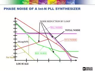
PHASE NOISE OF A Int -N PLL SYNTHESIZER
NOISE REDUCTION BY LOOP. PLL NOISE. TOTAL NOISE. VCO NOISE. 20Log(N/R). REF NOISE. Ref Noise. LOG SCALE. LOG SCALE. PHASE NOISE OF A Int -N PLL SYNTHESIZER. Noise Contributors in a Frac-N PLL. Example: 3 rd order MASH SD modulator, 3 rd order loop. “synth” noise. Ref. noise.
1.42k views • 2 slides
Phase Locked Loop Design
CSE598A/EE597G Spring 2006. Phase Locked Loop Design. KyoungTae Kang, Kyusun Choi Electrical Engineering Computer Science and Engineering. Frequency Synthesizer. General Synthesizer Issues. Frequency Spectrum. Settling Time (Lock Time). PLL Components Circuits. PLL Components Circuits.
1.04k views • 40 slides
EE311: Junior EE Lab Phase Locked Loop
EE311: Junior EE Lab Phase Locked Loop. J. Carroll 9/3/02. Background Theory. Phase locked loop (PLL) is a controlled oscillator whose instantaneous frequency is dynamically adjusted through feedback and filtering
399 views • 14 slides

The Design Of A Differential CMOS Charge Pump For High Performance Phase-Locked-Loops
The Design Of A Differential CMOS Charge Pump For High Performance Phase-Locked-Loops. 班級:積體所碩一 學生:林欣緯 指導教授:林志明 教授. Bortecene Terlemez and John P. Uyemura ISCAS2004. Outline. Introduction Charge Pump Architecture Simulation Results PLL Test Result Conclusion. Introduction.
684 views • 17 slides
Phase Locked Loop Design
Phase Locked Loop Design. Matt Knoll Engineering 315. Introduction. What is a PLL? Control System Representation Parts of a PLL PLL in Simulink. What is a PLL?. Digital frequency control system Generate high speed oscillations Acquire and track signals Radio Frequency Demodulation
345 views • 13 slides
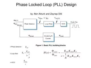
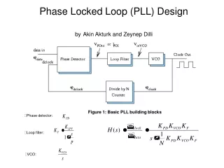
Phase Locked Loop (PLL) Design by Akin Akturk and Zeynep Dilli
Phase detector:. Loop filter:. VCO:. Phase Locked Loop (PLL) Design by Akin Akturk and Zeynep Dilli. Figure 1: Basic PLL building blocks. Phase Detector Design. Figure 2: Phase Frequency Detector and the Loop Filter. Figure 3: PD and Loop Filter responses to input transients.
498 views • 9 slides
PHASE LOCKED LOOP SIMULATIONS
PHASE LOCKED LOOP SIMULATIONS. By, R.Vikram Reddy(0104445). Talk Outline. History Introduction PLL Basics PLL Types Loop Components -Phase Detectors -Voltage controlled Oscillators -Loop Filters Applications.
1.43k views • 54 slides
SIMPLE PHASE LOCKED LOOP
SIMPLE PHASE LOCKED LOOP. PRESENTED BY :- Vivek Pathak (1409904) Abhishek Solanki (1409905) Varad Kinjal Pooja. What is PLL?. PLL = Phase Lock Loop
408 views • 15 slides
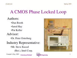
A CMOS Phase Locked Loop
A CMOS Phase Locked Loop. Authors: Dan Booth Jared Hay Pat Keller. Advisor: Dr. Peter Osterberg Industry Representative: Mr. Steve Kassel (Ret.), Intel Corp. Agenda. Introduction Dan Booth Background Dan Booth Methods Pat Keller Results Pat Keller Conclusions Jared Hay
598 views • 26 slides

Phase-Locked Loop
Phase-Locked Loop. Phase-Locked Loop in RF Receiver. Antenna. BPF1. LNA. BPF2. Mixer. BPF3. IF Amp. Demodulator. RF front end. LO. VCO. Ref. PD. Loop Filter. Phase-Locked Loop. 1/N. Functional Blocks in PLL. Phase detector (PD): find difference between phases of two signals
1.65k views • 72 slides
New Control Strategy for Three-Phase Grid-Connected LCL Inverters without a Phase-Locked Loop
The three-phase synchronous reference frame phase-locked loop (SRF-PLL) is widely used for synchronization applications in power systems. In this paper, a new control strategy for three-phase grid-connected LCL inverters without a PLL is presented. According to the new strategy, a current reference can be generated by using the instantaneous power control scheme and the proposed positive-sequence voltage detector. Through theoretical analysis, it is indicated that a high-quality grid current can be produced by introducing the new control strategy. In addition, a kind of independent control for reactive power can be achieved under unbalanced and distorted grid conditions. Finally, the excellent performance of the proposed control strategy is validated by means of simulation and experimental results.
123 views • 6 slides
Phase Locked Loop (PLL) Design by Akin Akturk and Zeynep Dilli
Phase detector:. Loop filter:. VCO:. Phase Locked Loop (PLL) Design by Akin Akturk and Zeynep Dilli. Figure 1: Basic PLL building blocks. Phase Detector Design. Figure 2: Phase Frequency Detector and the Loop Filter. Figure 3: PD and Loop Filter responses to input transients.
175 views • 9 slides
